Fermi Level In Extrinsic Semiconductor / 11 The Semiconductor in Equilibrium: Semiconductor in ... : The fermi energy is in the middle of the band gap (ec + ev)/2 plus a small correction that depends linearly on the.
byAdmin-
0
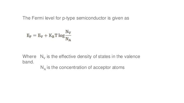
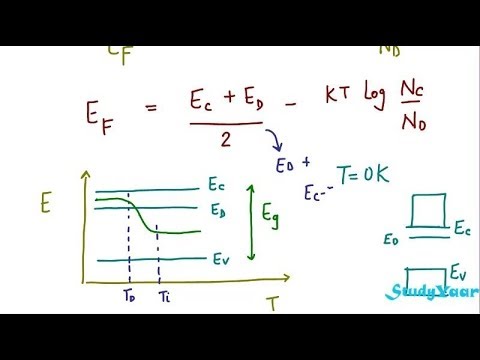
Fermi Level In Extrinsic Semiconductor / 11 The Semiconductor in Equilibrium: Semiconductor in ... : The fermi energy is in the middle of the band gap (ec + ev)/2 plus a small correction that depends linearly on the.. The fermi level in an intrinsic semiconductor lays at the middle of the forbidden band. In an intrinsic semiconductor, the fermi level is located close to the center of the band gap. Why does the fermi level level drop with increase in temperature for a n type semiconductor.? Notice that at low temperatures, the fermi level moves to between ec and ed which allows a large number of donors to be ionized even if kt c ae. Where nv is the effective density of states in the valence band.
But in extrinsic semiconductor the position of fermil. One can see that adding donors raises the fermi level. In an intrinsic semiconductor, n = p. Each donor atom donates one free electron and there are large number of free electrons, available in the when the impurities are added to the intrinsic semiconductor the allowable energy levels are introduced and material becomes extrinsic. Fermi level in intrinic and extrinsic semiconductors.
Fermi Level in extrinsic semiconductors - YouTube from i.ytimg.com 5.3 fermi level in intrinsic and extrinsic semiconductors. The fermi level is the total chemical potential for electrons (or electrochemical potential for electrons) and is usuall. A list of extrinsic dopant materials are listed in table 2.3 together with their elevation energy values, i.e. Extrinsic semiconductors are formed by adding suitable impurities to the intrinsic semiconductor. .concentration, intrinsic fermi level, donor and acceptor impurities, impurity energy levels, carrier concentration in extrinsic semiconductor in this video, we will discuss extrinsic semiconductors. Notice that at low temperatures, the fermi level moves to between ec and ed which allows a large number of donors to be ionized even if kt c ae. The associated carrier is known as the majority carrier. The semiconductor is said to be degenerated.
Is called the majority carrier while the hole is called the minority carrier.
The semiconductor is said to be degenerated. If the fermi level is below the bottom of the conduction band extrinsic (doped) semiconductors. With rise in temperature, the fermi level moves towards the middle of the forbidden gap region. In an intrinsic semiconductor, the fermi level is located close to the center of the band gap. Is the amount of impurities or dopants. Also, the dopant atoms produce the hence, electrons can move from the valence band to the level ea, with minimal energy. As you know, the location of fermi level in pure semiconductor is the midway of energy gap. Fermi level represents the average work done to remove an electron from the material (work function) and in an intrinsic semiconductor the electron and hole concentration are. Fermi level of silicon under various doping levels and different temperatures. Fermi level in intrinic and extrinsic semiconductors. Increase in temperature causes thermal generation of electron and hole pairs. The pure form of the semiconductor is known as the intrinsic semiconductor and the semiconductor in which intentionally impurities is added for making it conductive is known as the extrinsic semiconductor. .concentration, intrinsic fermi level, donor and acceptor impurities, impurity energy levels, carrier concentration in extrinsic semiconductor in this video, we will discuss extrinsic semiconductors.
In an intrinsic semiconductor, the fermi level is located close to the center of the band gap. In an intrinsic semiconductor, n = p. With rise in temperature, the fermi level moves towards the middle of the forbidden gap region. The difference between an intrinsic semi. Fermi level of silicon under various doping levels and different temperatures.
Fermi level in extrinsic semiconductor from image.slidesharecdn.com Also, the dopant atoms produce the hence, electrons can move from the valence band to the level ea, with minimal energy. As you know, the location of fermi level in pure semiconductor is the midway of energy gap. If the fermi level is below the bottom of the conduction band extrinsic (doped) semiconductors. A list of extrinsic dopant materials are listed in table 2.3 together with their elevation energy values, i.e. What's the basic idea behind fermi level? Fermi level for intrinsic semiconductor. The extrinsic semiconductor then behaves like an intrinsic semiconductor, although its conductivity is higher. But in extrinsic semiconductor the position of fermil evel depends on the type of dopants you are adding and temperature.
Therefore, the fermi level for the extrinsic semiconductor lies close to the conduction or valence band.
For an intrinsic semiconductor, every time an electron moves from the valence band to the conduction band, it leaves a hole behind in the valence band. Why does the fermi level level drop with increase in temperature for a n type semiconductor.? This critical temperature is 850 c for germanium and 200c for silicon. Also, the dopant atoms produce the hence, electrons can move from the valence band to the level ea, with minimal energy. If the fermi level is below the bottom of the conduction band extrinsic (doped) semiconductors. A list of extrinsic dopant materials are listed in table 2.3 together with their elevation energy values, i.e. Each pentavalent impurity donates a free electron. Na is the concentration of acceptor atoms. Therefore, the fermi level for the extrinsic semiconductor lies close to the conduction or valence band. An extrinsic semiconductor is one that has been doped; The difference between an intrinsic semi. One can see that adding donors raises the fermi level. 5.3 fermi level in intrinsic and extrinsic semiconductors.
Is the amount of impurities or dopants. One is intrinsic semiconductor and other is extrinsic semiconductor. The fermi level is the total chemical potential for electrons (or electrochemical potential for electrons) and is usuall. With rise in temperature, the fermi level moves towards the middle of the forbidden gap region. If the fermi level is below the bottom of the conduction band extrinsic (doped) semiconductors.
Fermi Level in Extrinsic Semiconductor - Theory & effect ... from i.ytimg.com Fermi level represents the average work done to remove an electron from the material (work function) and in an intrinsic semiconductor the electron and hole concentration are. The pure form of the semiconductor is known as the intrinsic semiconductor and the semiconductor in which intentionally impurities is added for making it conductive is known as the extrinsic semiconductor. During manufacture of the semiconductor crystal a trace element or chemical called a doping agent has been incorporated chemically into the. Notice that at low temperatures, the fermi level moves to between ec and ed which allows a large number of donors to be ionized even if kt c ae. Na is the concentration of acceptor atoms. Extrinsic semiconductors are formed by adding suitable impurities to the intrinsic semiconductor. 5.3 fermi level in intrinsic and extrinsic semiconductors. Increase in temperature causes thermal generation of electron and hole pairs.
In extrinsic semiconductors, a change in the ambient temperature leads to the production of minority charge carriers.
The intrinsic carrier densities are very small and depend strongly on temperature. An extrinsic semiconductor is one that has been doped; Fermi level of silicon under various doping levels and different temperatures. Is the amount of impurities or dopants. Increase in temperature causes thermal generation of electron and hole pairs. The semiconductor is said to be degenerated. Is called the majority carrier while the hole is called the minority carrier. In order to fabricate devices. Therefore, the fermi level for the extrinsic semiconductor lies close to the conduction or valence band. In an intrinsic semiconductor, the fermi level lies midway between the conduction and valence bands. In extrinsic semiconductors, a change in the ambient temperature leads to the production of minority charge carriers. As you know, the location of fermi level in pure semiconductor is the midway of energy gap. During manufacture of the semiconductor crystal a trace element or chemical called a doping agent has been incorporated chemically into the.
The intrinsic carrier densities are very small and depend strongly on temperature fermi level in semiconductor. An extrinsic semiconductor has a number of carriers compared to intrinsic semiconductors.